mainmenu
To explore new physics phenomena of low dimensional materials
with a special emphasis on two-dimensional layered structures
[News] Understanding the Impact of Defects on the Properties of MoS2
- WriterCenter for Integrated Nanostruture Physics
- RegDate2017-12-21
- Hit10716
- att.
내용보기
Understanding the Impact of Defects on the Properties of MoS2
- Highly desired in the petrochemical industry, but generally unwanted in electronics manufacture, defects in MoS2 influence the properties and utility of this material. Analysis of atomically thin MoS2 reveals how defects behave and relate to MoS2’s anomalies -
Researchers at the Center for Integrated Nanostructure Physics, within the Institute for Basic Science (IBS), have shown that defects in monolayer molybdenum disulfide (MoS2) exhibit electrical switching, providing new insights into the electrical properties of this material. As MoS2 is one of the most promising 2D semiconductors, it is expected that these results will contribute to its future use in opto-electronics.
Defects can cause major changes in the properties of a material, leading to either desirable or unwanted effects. For example, petrochemical industry has long taken advantage of the catalytic activity of edges of MoS2, caused by the presence of a high concentration of defects, to produce petroleum products with reduced sulfur dioxide (SO2) emissions. On the other hand, having a pristine material is a must in electronics. Currently, silicon rules the industry, because it can be prepared in a virtually defect-free manner. In the case of MoS2, its suitability for electronic applications is currently limited by the presence of naturally occurring defects. So far, the precise link between these defects and the degraded properties of MoS2 has been an open question.
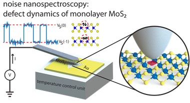
In IBS, a team of physicists, material scientists, and electrical engineers worked closely together to explore the electronic properties of sulfur vacancies in MoS2 monolayers, using a combination of atomic force microscopy (AFM) and noise analysis. The scientists used a metallic AFM tip to measure the noise signal, i.e., the variation of electrical current passing through a single layer of MoS2 placed on a metal substrate.
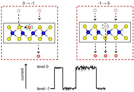
The most common defects in MoS2 are instances of missing single sulfur atoms, also known as sulfur monovacancies. In a perfect sample, each sulfur atom has two valence electrons that bind to two molybdenum electrons. However, where a sulfur atom is missing, these two molybdenum electrons are left unsaturated, defining the neutral state (0 state) of the defect. However, the team observed rapid switching events in their noise measurements, indicating the state of the vacancy switched between neutral (0 state) and charged (-1 state). “The switching between 0 and -1 is happening continuously. While an electron resides at the vacancy for a while, it is missing from the current, such that we observe a current drop,” explains Michael Neumann, one of the co-first authors of the study. “This goes a long way towards understanding the known anomalies of MoS2, and it is very interesting that sulfur vacancies alone are enough to explain these anomalies, without requiring more complex defects." According to the experiments and earlier calculations, two electrons can be also trapped at the vacancy (-2 state), but this does not seem to be energetically favored.

▲ Figure 1Experimental design. The study on 2D molybdenum disulfide (MoS2) defects employed low frequency noise measurements and conductive atomic force microscopy (C-AFM). The enlarged image shows an AFM cantilever tip pointing to an area with one sulfur monovacancy (area shaded red). As current flows through the AFM tip and the sample, switching events between different ionization states (neutral and charged -1) are measured. With a radius of around 25 nanometers, the AFM tip covers an area that contains around 1-8 sulfur monovacancies.

▲ Figure 2Dynamics of a sulfur vacancy. The top graph illustrates the switching processes between the neutral level (0 state) and the charged level (-1 state) that occur when an electron (red circle) from the flowing current is trapped (top left) or released (top right) at the sulfur vacancy defect (marked by green circle). The lower graph shows switching events in the current that occur when electrons from the current passing through the MoS2 sample are trapped at the vacancy, or released from the vacancy.
The new observation that sulfur vacancies can be charged (-1 and -2 states) sheds light on several MoS2 anomalies, including its reduced electron mobility observed in MoS2 monolayer samples: electrons move following the direction of an applied voltage, but get scattered by charged defects. “The -1 state is occupied around 50% of the time, which would lead to scattering of electrons, and thus explain why MoS2 has such poor mobility,” clarifies Neumann. Other MoS2 characteristics which can be explained by this study are the n-type doping of MoS2, and the unexpectedly large resistance at the MoS2-metal junction.
"This research opens up the possibility of developing a new noise nanospectroscopy device capable of mapping one or more defects on a nanoscale scale over a wide area of a 2D material," concludes the corresponding author Young Hee Lee.
The full study is available on Nature Communications.
Letizia Diamante
Notes for editors
- References
Seung Hyun Song, Min-Kyu Joo, Michael Neumann, Hyun Kim, Young Hee Lee. Probing defect dynamics in monolayer MoS2 via noise nanospectroscopy. Nature Communications (2017). DOI: 10.1038/s41467-017-02297-3
- Media Contact
For further information or to request media assistance, please contact: Mr. Shi Bo Shim, Head of Department of Communications, Institute for Basic Science (+82-42-878-8189, sibo@ibs.re.kr); Mr. Jung Gyu Kim, Global Officer, Department of Communications, Institute for Basic Science (+82-42-878-8172, jungkki1@ibs.re.kr); or Dr. Letizia Diamante, Science Writer and Visual Producer (+82-42-878-8260, letizia@ibs.re.kr).
- About the Institute for Basic Science (IBS)
IBS was founded in 2011 by the government of the Republic of Korea with the sole purpose of driving forward the development of basic science in South Korea. IBS has launched 28 research centers as of January 2017. There are nine physics, one mathematics, six chemistry, eight life science, one earth science and three interdisciplinary research centers.


